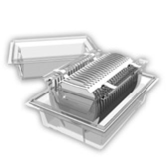
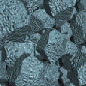
Poly-Crystaline Silicon (Nuggets)

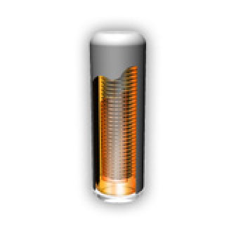
Pulling Single Crystal Silicon Ingots (CZ Method)
Polycrystalline silicon is put into a quartz crucible and heated and melted by a graphite heater under reduced pressure in an inert atmosphere.
After that, seed crystals are dipped into the surface of the melt, and silicon single-crystals are grown while controlling the pulling speed of the crystals and the temperature inside the furnace.
CZ method : Czochralski method
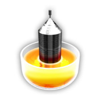

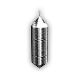
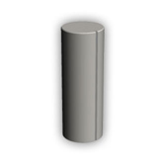
Image of Single Crystal Silicon Ingots
The single-crystal silicon ingot has a cylindrical shape as shown in the figure.
Crystals for φ300 mm wafers are very large, measuring 2 m in length and weighing over 300 kg.

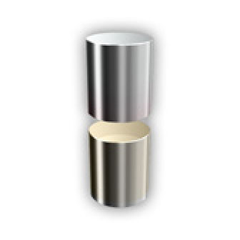
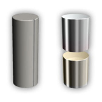
Peripheral Grinding
The outer circumference of a single crystal silicon ingot is ground to a specified diameter.
A part of the periphery is processed to form grooves (notches) or planes (orientation flats) to indicate the crystal orientation.
The figure shows the formed groove (notch).
After that, it is cut to the specified length before slicing.

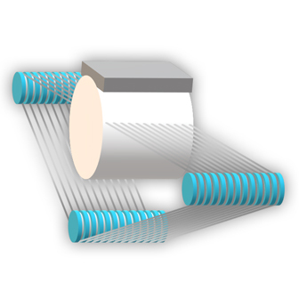
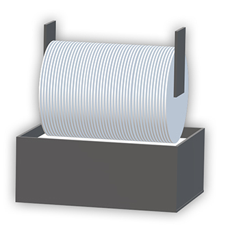
Slicing
Ingots are cut into wafers by using either the wire saw method or the internal blade method.
The figure shows the wire saw method.

Beveling (Peripheral Rounding)
To prevent chipping and cracking during the wafer fabrication process, the edge of the wafer is ground and chamfered in an arc shape with a diamond wheel.

Lapping (Double Side Lapping)
Wafers are set in a carrier, which spins between two rotating lapping plates. Both surfaces of the wafers are lapped to remove damaged surface layer and to achieve predetermined uniform thickness.


Etching (Chemical Polishing)
To completely remove the fracture layer caused by the machining process, etching is performed with acid or alkali chemicals.

Polishing (mirror polishing)
The wafer is pressed against a surface plate covered with an abrasive cloth.
The surface of the wafer is polished to a mirror finish by a combined mechanical and chemical treatment while applying an abrasive.

Annealing Treatment
High-temperature heat treatment is performed in a vertical furnace to eliminate void defects generated during crystal growth.
At the same time, oxygen precipitates are formed inside the wafer.

Cleaning
Wafers are physically and chemically cleaned using ultra-pure water and chemicals.

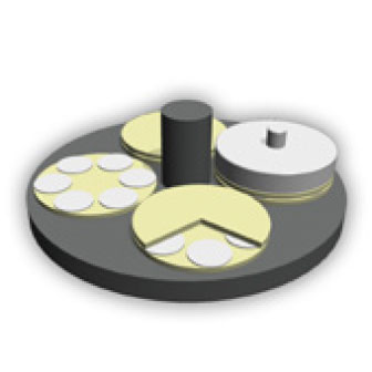
Inspections
Numerous inspections are performed, to check flatness, particles, impurity concentration, specific resistance, etc.


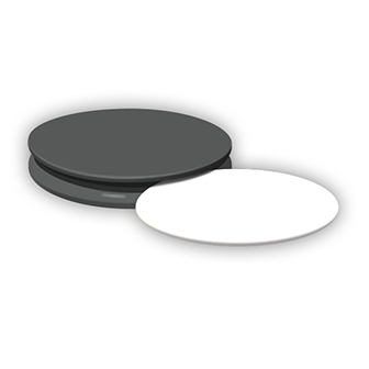
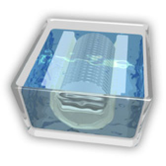
Packaging
Wafers are packaged in a clean shipping case, and sealed in a special moisture-proof bag.