About Sllicon wafer
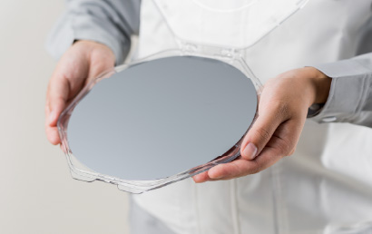
Silicon wafers, used as components of semiconductor devices, are thin disks (wafers) cut from high-purity silicon.
The silicon is formed into a cylindrical mass, the ingot is cut out to a thickness of about 1 mm, and the process of cleaning and polishing is applied to the surface to complete the process.
Silicon Wafers and Society
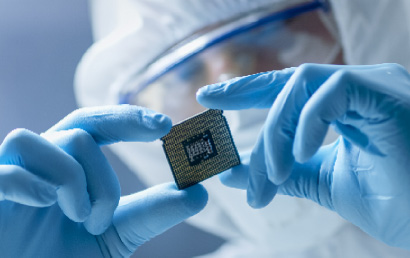
Semiconductor devices are used in all kinds of electronic equipment, small and large, including information terminals, home appliances, and large vehicles that exist in our daily lives.
It is no exaggeration to say that silicon wafers, components that serve as the substrate for those devices, are now part of our daily lives.
Silicon Wafers and Globalwafers Japan
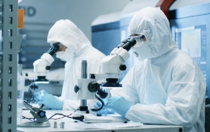
The advance of silicon wafer research and development to date has been very rapid.
We take the use of many high-performance electronic devices for granted, but behind our daily lives is a strong link between the improved quality and lower cost of these silicon wafers.