"ECAS®" Series Engineered Wafer
"Flexible customization according to purposes of use" based on GWJ's unique heat treatment technology
ECAS® wafer is silicon wafer products developed for advanced semiconductor devices.
They were produced through innovative development of crystal technologies and heat treatment process technologies, and can be customized for customer devices.
In addition, the development of processing technologies has resulted in improved flatness.
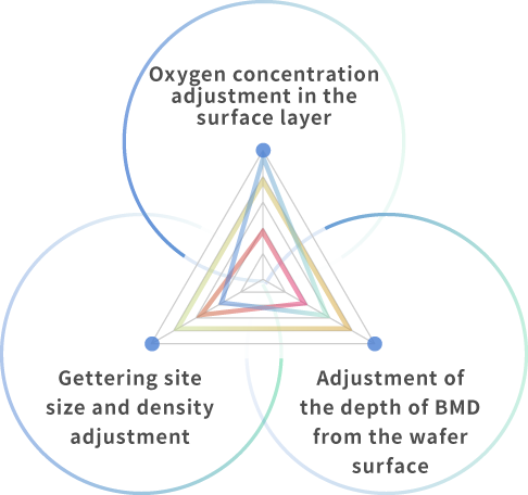
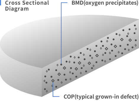
About ECAS® Wafer Heat Treatment Technology
GlobalWafers Japan can design wafers according to each client's requirements.
| Heat treatment technology for ECAS® Wafer | Benefits from processing |
|---|---|
| Gettering site size and density adjustment | Improved ability to capture (gettering) metallic impurities that contaminate products during clients' processing steps. |
| Adjustment of the depth of BMD (Bulk Micro Defect) from the wafer surface | It is possible to improve yield by forming defect-free and gettering layers suited for each client's device. |
| Adjustment of the width of the defect-free area on the wafer surface | Higher oxygen concentration improves wafer strength. |
-
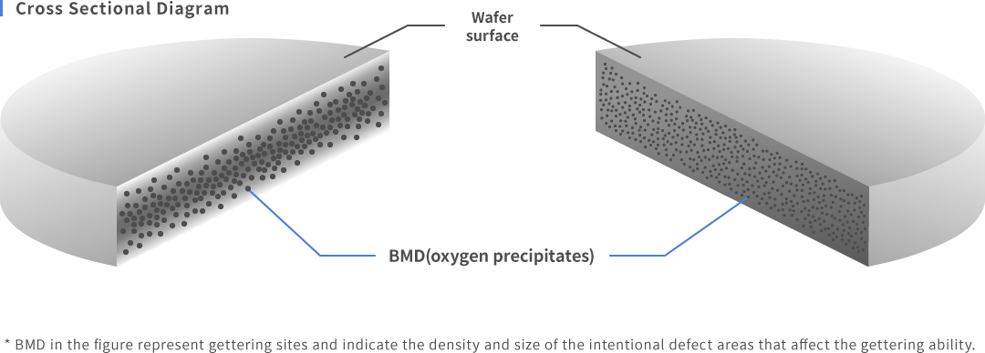
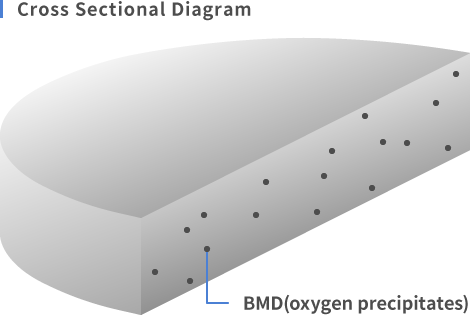
Gettering site size and density adjustment
Heat treatment technology allows us to freely adjust the size and density of the gettering sites as requested.
-
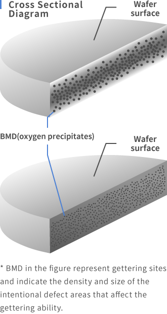
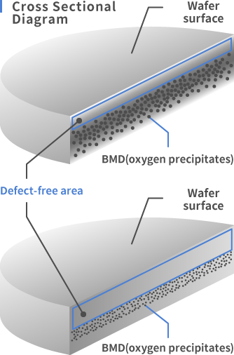
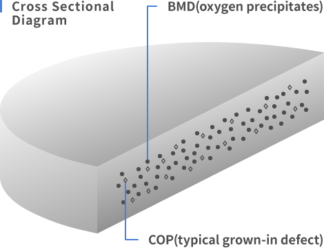
Adjustment of the depth of BMD (Bulk Micro Defect) from the wafer surface
The width from the wafer surface to the gettering site (defect-free area) can be adjusted by our heat treatment technology.
-
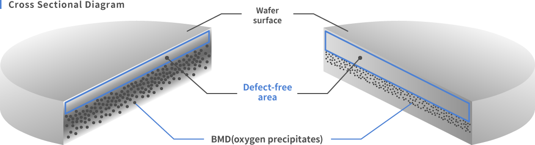
Oxygen concentration adjustment in the wafer surface layer
The oxygen concentration of the surface layer can be adjusted as required with the heat treatment technology.
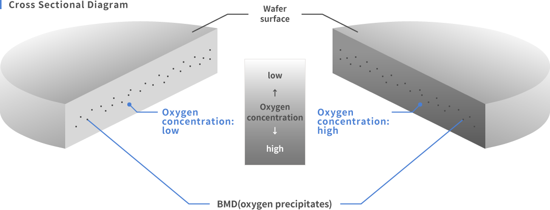
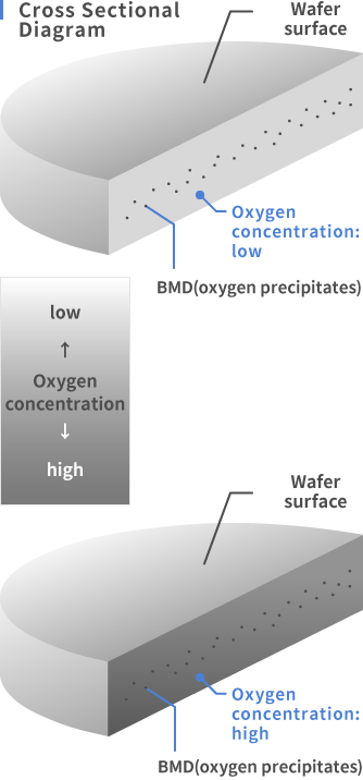
- * The black and white shading in the figure represents oxygen impurity concentration.
- * Oxygen concentration at the depth of several μm to several 10 μm in the wafer surface layer is controlled by our heat treatment technology.
- * The oxygen concentration inside the wafer (bulk) is controlled by our crystal growth technology.
Polished Wafer
Polished wafers are silicon wafers that are mirror-polished on one or both sides.
GlobalWafers Japan's polished wafers, with excellent characteristics such as high flatness, high cleanliness, and proper gettering, have earned a reputation as high quality, high precision products that meet the needs of advanced memory devices, etc.
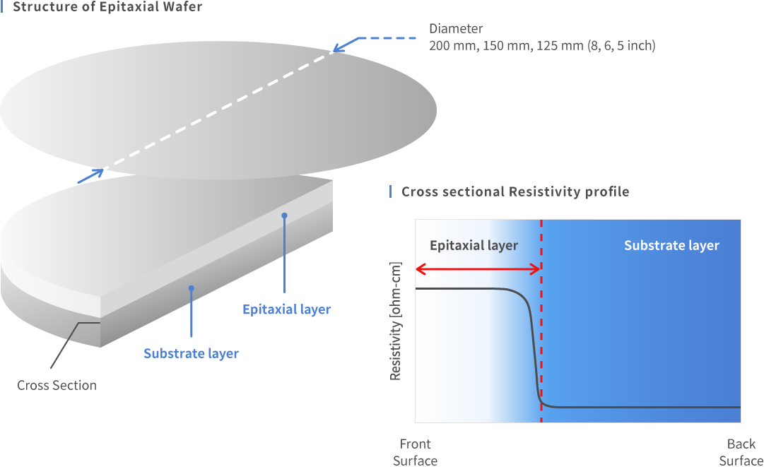
Epitaxial Wafer
Epitaxial wafers, for which silicon single crystals of the required specifications are grown on the surface of polished wafers from the vapor phase, are used for individual devices such as transistors and diodes, as well as for bipolar and MOS-type IC substrates.
GlobalWafers Japan meets a wide range of demand for epitaxial wafers with multilayer structures, including embedded diffusion wafers.
In particular, power devices on which we focus are often used in devices that control power, and contribute to more efficient energy use.
Hi-WAFER®
Hi-WAFER® (hydrogen annealed wafers) are hydrogen-treated to achieve high internal gettering capability and COP-free wafer surfaces. These characteristics provide the wafers with excellent oxide film properties.
Hyper Hi-WAFER®
Hyper Hi-WAFER® (hydrogen annealed wafers) were developed for cutting-edge devices.
The improved crystalline technology, optimized hydrogen treatment, and improved processing techniques have resulted in improved internal gettering and flatness properties compared to conventional Hi-WAFER®, as well as reduced LSTD density.
Electrical characteristics such as junction leakage characteristics have been further improved compared to conventional silicon wafers as well as Hi-WAFER®.
They also have excellent flatness characteristics to allow miniaturization.
Wafers for advanced miniaturized products contribute to the miniaturization of LSI devices, and device process miniaturization contributes to energy saving in the form of lower operating voltage.
AT-Wafer
AT wafer (argon annealed wafers) is high-quality substrates treated with argon to achieve both a defect-free surface and excellent internal gettering capability.
Like Hyper Hi-WAFER®, these wafers were developed for use in miniaturized devices and feature a flat boron profile around the surface.
Wafers for advanced miniaturized products contribute to the miniaturization of LSI devices, and device process miniaturization contributes to energy saving in the form of reduced operating voltage.
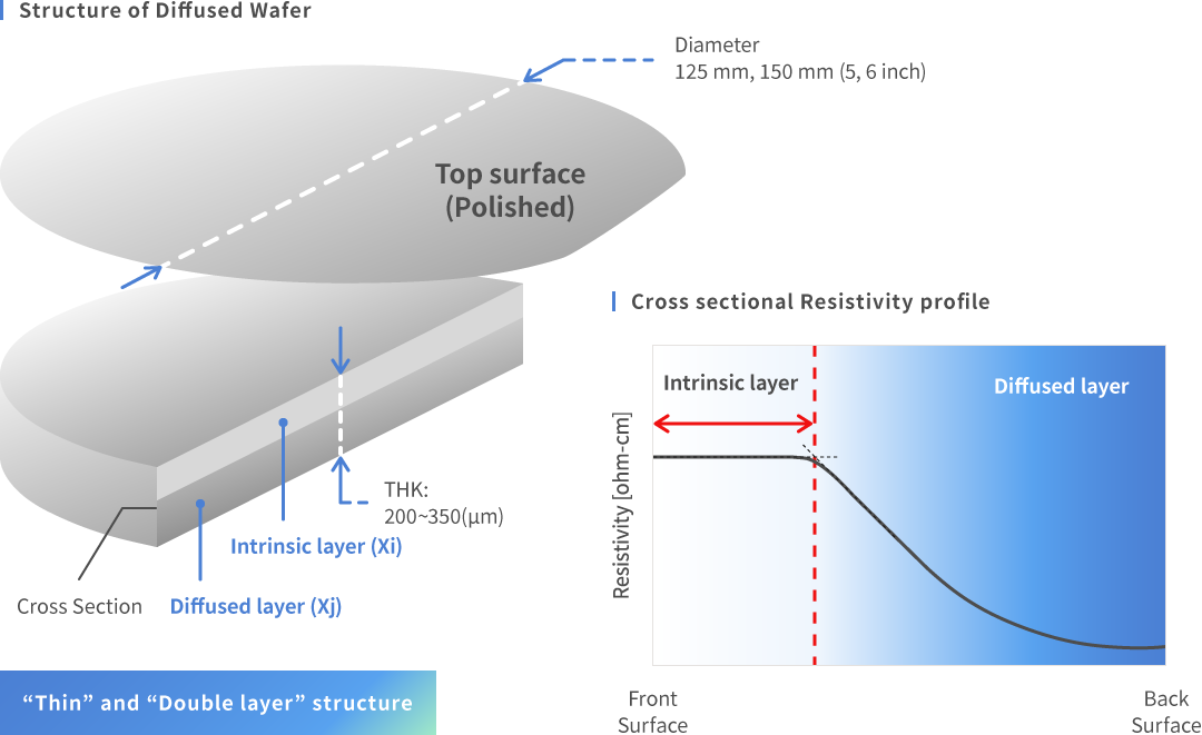
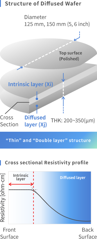
Diffused Wafer
Diffused wafer is employed in electric power control devices frequently and contribute to improving the efficiency of energy consumption.
Our Diffused Wafers which ensured accurate diffusion concentration, diffusion depth and undiffused width through precisely controlled process are easy for users to control in the manufacturing process and offer superior products with favorable conditions for device design has been well received as.
General Specification for Diffused Wafer
Detail and further requirements need to be confirmed individually.
Please contact us.
| Item | Diameter | |||
|---|---|---|---|---|
| φ5″ | φ6″ | |||
| Structure | N-/N+, N-/P+, P-/P+ | |||
| Crystal Growing Method | MCZ, CZ, FZ | |||
| Crystal Orientation | (100), (111) | |||
| Type of Intrinsic layer (Dopant) | N(Phos, Phos(NTD)), P(Boron) | |||
| Type of Diffusion (Dopant) | N+(Phos.), P+(Boron) | |||
| Diffused Layer (Xj) | Depth | (μm) | 50 ~ 250 | |
| Tolerance | (μm) | ±10 | ||
| Undiffused Layer (Xi) (Intrinsic Layer) | Width | (μm) | 20 ~ 300 | |
| Tolerance | (μm) | ±5 | ||
| Wafer Thickness | Thickness | (μm) | 200 ~ 350 | |
| Tolerance | (μm) | ±15 | ||
| Warp-bf | (μm) | ≦250 | ≦300 | |
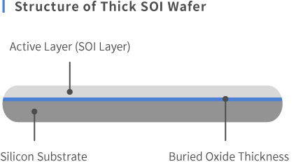
Thick SOI Wafer
Thick SOI wafers have widely been used in power devices and also high performance of MEMS.
The demand for Thick SOI wafers such as intelligent power modulus which require high breakdown voltage and low energy consumption is increasing. MEMS made of Thick SOI wafers bring complex 3-D structure such as accelerometer, pressure sensor and so on.
The thick SOI wafers we produce are manufactured with the bonding method and are controlled the thickness of active layer and BOX layer precisely to respond various customized requirements.
Features of Our Thick SOI Wafers
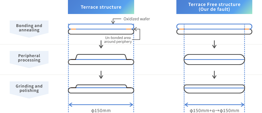
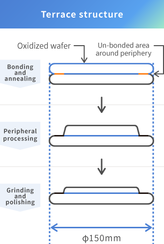
Ordinary bonded Thick SOI wafers took the "Terrace structure" in order to remove un-bonded area around periphery of wafer. This terrace sometimes may cover up to approximately 10% area of the wafer surface.
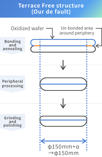
GlobalWafers Japan has been able to provide Thick SOI wafers without the "Terrace" so called "Terrace Free structure" by controlling diameter of both substrates.
This unique structure can help customers handle the Thick SOI wafers on the same processing as regular wafers, and consequently give larger device manufacturing area for in a wafer.
General spec
*1 Need to be discussed for (111) and (110) individually.
*2 Only condition for 150mm Diameter, ≧400μm Handle wafer, Polished backside, without backside oxide.
*3 ±10% tolerance for Box≦0.5μm. Need to be discussed individually for the case of Box > 2.0μm.
Detail and further requirements need to be confirmed individually.
Please contact us.
| Item | |||||
|---|---|---|---|---|---|
| 100mm | 125mm | 150mm | |||
| Surface orientation | (100), (111)*1, (110)*1 | ||||
| Type(Dopant) | N(Phos., Sb), P(Boron) | ||||
| Active layer thickness | (μm) | 3.0~300.0 | |||
| Active layer thickness (Tolerance) |
(μm) | ±0.5 (Standard Process) | |||
| ±0.3 (High precision process only) *2 | |||||
| Buried oxide thickness | (μm) | ≦2.0 *3 | |||
| Buried oxide thickness (Tolerance) |
(%) | ±5.0 *3 | |||
| Handle wafer thickness | (μm) | 250~625 | |||
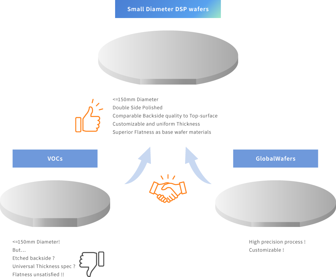
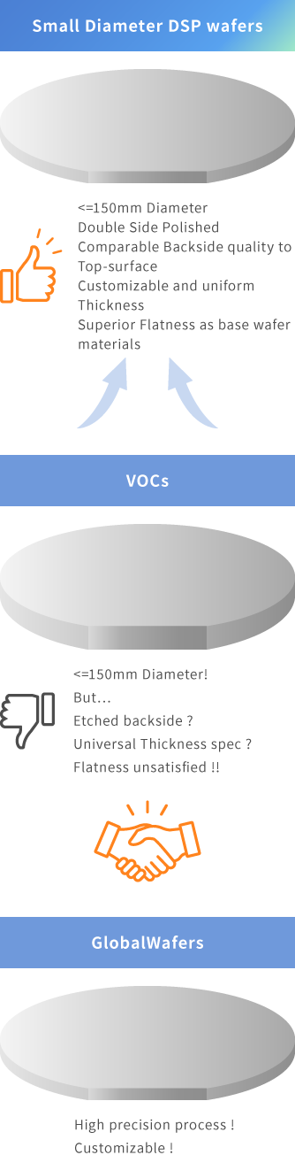
Small diameter DSP (Double Side Polished) Wafer
For small-diameter wafers conventionally, chemical etched backside has been the global standard for semiconductor use.
In recent years, we have received requests from customers who want thin wafers and also need the equivalent polishing quality on the backside as the top surface for various sensing devices like detectors, or customers who want superior flatness for substrate materials for MEMS, SAW filter devices.
To respond such VOCs, we applied the high-precision processing technology that we have cultivated through production of the diffused wafers and the thick SOI wafers, the double-side-polished wafers with <=150mm Diameter and superior flatness have been commercialized.
For the crystals, the Czochralski method (CZ, MCZ) which is the most common for silicon single crystals, and also the float zone method (FZ) which can be achieved extremely low interstitial oxygen concentration and ultra high resistivity are available to be provided.
General specification
* Depending on individual spec, quality assurance by using monitor wafers may be applied.
Detail and further requirements need to be confirmed individually.
Please contact us.
| Item | |||||
|---|---|---|---|---|---|
| General Specifications | |||||
| Diameter | 100mm, 125mm, 150mm | ||||
| Crystal growth method | CZ, MCZ, FZ | ||||
| Crystal orientation | (100), (111) | ||||
| Conductivity type (Dopant) | N(Phos., Phos.(NTD), Sb) | ||||
| P(Boron) | |||||
| Wafer thickness | (μm) | 300~1000 * | |||
| Wafer thickness (Tolerance) | (%) | ±10.0 * | |||
| TTV | (μm) | ≦1.0 * | |||
Product Line
| Product Name | Type | Purpose of Use | 100mm | 125mm | 150mm | 200mm | 300mm |
|---|---|---|---|---|---|---|---|
| Polished Wafer | "ECAS®" Series Engineered Wafer | Memory(DRAM,NAND)/Logic/ Analog/Image Sensor/IGBT |
〇 | ||||
| CZ-Wafer | 〇 | 〇 | |||||
| FZ-Wafer | IGBT/Diode | 〇 | |||||
| DSP Wafer | Detector/MEMS/SAW device | 〇 | 〇 | 〇 | |||
| Annealed Wafer | Hi-WAFER® | Memory(DRAM,NAND)/Logic/ Analog/Image Sensor |
〇 | ||||
| Hyper Hi-WAFER® | 〇 | ||||||
| AT-Wafer | 〇 | 〇 | |||||
| Epitaxial Wafer | N/N+(As,Sb,Phos) | Discrete Devices/Small Signal/ Pw Transistor/IGBT/Bipolar IC |
〇 | 〇 | 〇 | ||
| P/P+ | 〇 | 〇 | 〇 | ||||
| N/P | 〇 | 〇 | 〇 | ||||
| N/N+/P+ | 〇 | 〇 | 〇 | ||||
| N/P BL=N+P+ | 〇 | 〇 | |||||
| P/P- | Memory(DRAM,NAND)/Logic/Analog/ Image Sensor |
〇 | |||||
| Diffused Wafer | N-/N+ | Pw Transistor/IGBT/ Diode/Transistor |
〇 | 〇 | |||
| P-/P+ | 〇 | 〇 | |||||
| N-/P+ | Pw Transistor/IGBT | 〇 | 〇 | ||||
| Thick SOI Wafer | N/SiO2/N | MEMS/Power Devices | 〇 | 〇 | 〇 | ||
| P/SiO2/P | 〇 | 〇 | 〇 |
Personal information received from customers will be used only for
responding to inquiries.
Please note that inquiries received on Saturdays, Sundays,
national holidays, year-end and New Year holidays, and other company
holidays will be answered on the next business day or later.