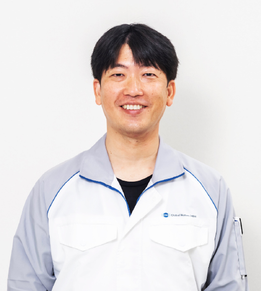
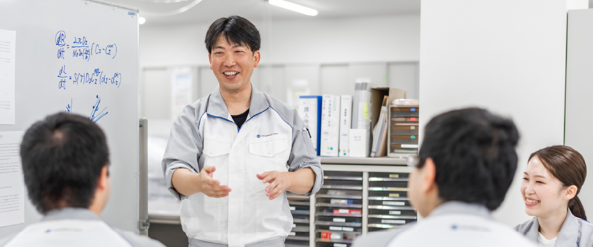
Advantage of GWJ - Annealing Technology Supervisor of Annealing Technology, Base Fundamental Technology Group, Technology Department Haruo Sudo
I am mainly in charge of research and development of annealing technology in the Technology Department.
GlobalWafers Japan (GWJ) possesses two types of annealing technology.
One is called “furnace batch annealing” and the other is called “rapid thermal process (RTP).”
One day, after having introduced RTP tools and beginning work on various experiments, our group discovered a unique phenomenon occurring during processing at a certain temperature.
The way in which this discovery caused a revolution in our silicon wafer manufacturing technology is the most memorable thing to ever happen to me at work.
(Doctoral Thesis)
My career as an engineer started from an encounter with unique annealing technology
I earned my master’s degree from Yamagata University.
My research theme at that time was “organic and inorganic composite materials.” This research involved changing the state of substances by applying heat treatment.
Once I had completed my master’s degree and it was time to decide on my future career path, my encounter with Globalwafers led to my interest in hydrogen annealing technology. Although the materials used in this technology differed from my research, I found it interesting due to the common theme of changing the state of silicon wafers through heat treatment.
At the same time as my encounter with the company, I also heard about a product for which impurities are mixed into silicon wafers and then diffused inside of the wafers.
However, I was initially skeptical regarding the reason for adding impurities to silicon wafers, which require high purity.
In fact, I asked the following question during my job interview: “Why put impurities into a silicon wafer that requires high purity?”
I was deeply moved by the kind and easy-to-understand responses to my question. It was then that I first imagined myself having a career at this company.
Annealing technology is an important and unique technology for added value in silicon wafers
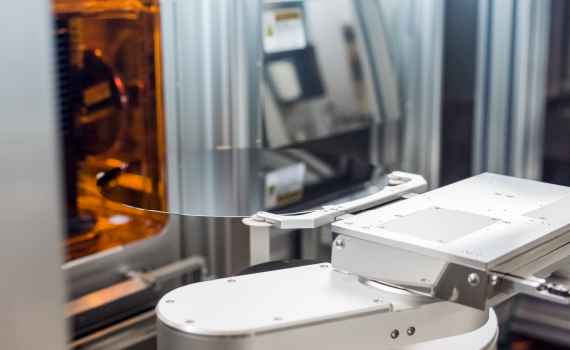
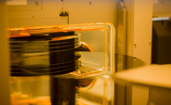
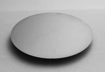
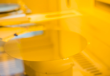
Manufacturing of silicon wafers begins with melting blocks of polysilicon and growing it into monocrystalline silicon. Single-crystal silicon is pulled out as a single-crystal silicon ingot with a diameter of 200 to 300 mm and a total length of more than 1 meter. The ingot is cut into thin slices to form silicon wafers. However, the inside of the silicon wafer at this stage is actually full of defects and cannot be said to be of high quality, despite being single-crystal silicon. The core of annealing technology is control via heat treatment in order to eliminate these defects and create new added value. Device manufacturers use silicon wafers that have been commercialized through annealing technology and add various processes to create high-quality semiconductors. We uses heat treatment technology to simultaneously implement a series of controls for improving the quality of silicon wafers. This is the annealing technology that is the strength of us.

Preventing unintended diffusion of impurities to the surface layer and controlling strength while simultaneously eliminating defects
For example, if metal impurities adhere to a silicon wafer, the metal impurities diffuse into the silicon wafer during the subsequent heat treatment process.
If the metal impurities exist on the silicon wafer surface layer, the semiconductor using this silicon wafer will cause device failure.
Therefore, there is a technology called “gettering” that traps metal impurities deep in the silicon wafer (capture/movement control) and prevents the impurities from manifesting on the surface layer.
The use of this technology to create silicon wafers with extremely high surface cleanliness is one example of added value provided to annealed wafers.
It is also possible to increase the mechanical strength even though it is a single crystal.
Above all, I believe that our greatest strength lies is how we are able to eliminate defects in single crystals while at the same time improving cleanliness and heightening strength.

Our future depends on growth of the Technical Department
I believe that growth of our Technology Development Department is essential in order to survive competition with other companies based on advanced technology.
In order for the Technology Development Department to grow, it is necessary for each and every employee to grow.
In that sense, technological development is an extremely interesting pursuit.
We and other current leading companies were able to establish their position based on the technology accumulated by our predecessors, not on the ability of people in my own generation.
When looking ahead to the future, it is imperative for us to develop and construct technology that will support the next generation.
When I had just begun working at this company, I remember a senior employee chuckling and saying “I don’t expect much from new hires.”
I was also told that “new employees can’t fail; they can only gain experience.” This way of thinking allowed me to freely take on a variety of experiments and research.
These experiences molded me into the engineer who I am today.
In 2021, I obtained my Working Professional Doctoral Degree (Ph.D.).
I was able to take on the challenge of acquiring this advanced degree thanks to the culture of the Technology Department that had been established by many senior employees. Another factor was my desire to acquire expert knowledge of technology for passing on to the next generation.
Right now, through technological development and research, I would like to continue building the ability to succeed in business for us.
*Departments and titles current as of the time of the interview