New Product Development Technical Director (Fellow Specialist), Technical Department Koji Izunome
Since joining the GlobalWafers Japan, I have worked in the Technology Department and handled technological development that leads to the development of new products.
Later in my career, I served as manager and general manager overseeing the Technological Department. After that, I assumed the position of executive officer in charge of technology.
I currently serve as Technical Director, a position which is also known as a Fellow. In this role, I handle tasks such as supporting the Technical Department and creating a roadmap for introducing next-generation technology.
Based on my experience, I would like to discuss some aspects of technological development capable of competing on a global scale.
Our current flagship products is an image of the future envisioned 15 years ago
So far, I have succeeded in developing and introducing three new products, or new technologies, at our company.
Of course, I was not solely responsible for any of these products. If new products and new technologies have a “creator” and a “cultivator,” then I would describe my role as that of the creator.
One of my creations is a product group called ECAS Series, which is currently our flagship product. My experience of being involved with the development of basic technologies of these products is the most memorable thing.
The shortest time frame for development of new products and new technology is around five years. Development with a long time frame may require around fifteen years.
The core technology used in the ECAS Series is based on an idea that I conceived about fifteen years ago.
I was overjoyed when my idea finally achieved success after fifteen years.
Properties of silicon crystals are like the Japanese archipelago
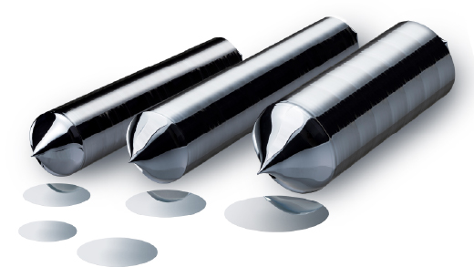
Have you ever seen a silicon crystal (ingot) before processing?
Silicon crystals are mined from the ground as very large chunks which resemble tuna caught in the port of Oma.
In fact, silicon wafer crystal has different properties (backgrounds) at all areas from top to bottom.
It is easy to imagine the myriad of properties in the crystals is you imagine the differences in the Japanese archipelago which stretches from Hokkaido to Kyushu and Okinawa.
Technology for creating uniform backgrounds
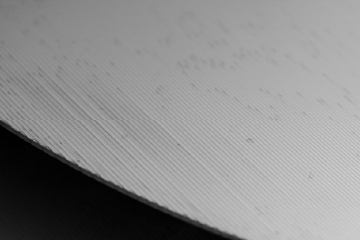
These crystals are thinly sliced and processed into products called silicon wafers. Continuing to use my metaphor of the Japanese archipelago, it is impossible to achieve stable products if Hokkaido is kept as Hokkaido and Kyushu is kept as Kyushu.
In response, I worked on a new technology for processing silicon wafers with different backgrounds and arranging them in an arbitrary state.
By realizing this new technology, We are now able to provide silicon wafers customized to the properties required by our customers.
We were able to achieve such a dramatic leap forward thanks to the unparalleled technology development department at our company, as well as to combined efforts of each department serving as creators who introduce new technologies to factories.

With a global perspective, making further advancements through our technological development capability
Although I serve as leader at the Technology Department, I actively encourage my subordinates to obtain doctoral degrees for working professionals.
I value doctoral degrees because collaboration with global academic research fields is the key to technological development of silicon wafers.
For this reason, Our employees are actively involved in the publication and presentation of academic papers in collaboration with academic societies and research institutes both in Japan and overseas.
When presenting such papers, the question often arises as to whether or not the presenter is a doctor (holds a Ph.D.), which can affect subsequent collaboration and exchange of information. This is especially true overseas.
We must have a broad global perspective, absorb the latest trends in areas such as technology, and incorporate those trends into our own development of new technology.
Doing so provides our employees with a real sense that our company possesses a competitive advantage and that we can succeed in global business.
I hope to further enhance the functionality of this cycle, and to create the optimal research and development environment for the many engineers at our company.
*Departments and titles current as of the time of the interview