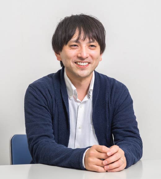
New Technology - AI In charge of AI Technology, Base Technology Group, Technology Dept. Yuta Nagai
There are so many different technical areas in the silicon wafer industry.
Crystal growth, processing, cleaning, and annealing technologies are typical examples, but I wanted to have core prowess that would give me confidence as an engineer, so I took on the challenge of obtaining a doctorate (PhD) while working.
Currently, as a new endeavor, I am focusing on the use of AI in the silicon wafer manufacturing process to realize smart factories.
Through these efforts, I hope to make GWJ and the silicon wafer manufacturing field an exciting company and industry.

Utilization of AI in the Rapidly Evolving Silicon Wafer Industry
In the silicon wafer and semiconductor industry, which continues to evolve and change at a dizzying and tremendous speed, I feel that the sense of speed demanded by our customers is "approaching a completely different dimension than in the past." In addition, the quality requirements for wafers set by our customers are becoming more demanding year by year.
Under such circumstances, I was concerned that it would become difficult to achieve the required speed and quality level if we continued the same technological development and product improvements as in conventional methods.
Therefore, the starting point was the idea of developing AI to assist technological development, in addition to the conventional development of new products and processes by engineers.
How AI is being used in the silicon wafer manufacturing process
In recent years, the manufacturing industry has been rapidly moving toward smart factories utilizing AI in areas such as quality control and production management. Our company is focusing its efforts on the use of AI for the silicon wafer manufacturing process. This falls under the research area of "process informatics (PI)."
The silicon wafer manufacturing process includes many processes, such as growing single crystal ingots, wafer processing, heat treatment, and epitaxial growth, and there are many requirements for quality, productivity, yield, etc. to be met for each of these processes.
In this context, we are working to utilize AI to develop process conditions to produce more silicon wafers of higher quality and more efficiently. As disclosed in our paper and press release, we have succeeded in an experiment in which we used AI to optimize the process conditions for epitaxial growth, thereby raising production efficiency about two times.
Through these efforts, I hope that AI can assist engineers in the development of next-generation processes, which have conventionally been conducted by engineers through experiments and computer simulators, thereby dramatically increasing the speed of technological development.
If you are interested, please take a look at our paper and press release.
Improvement of Material Development Speed" RIKEN GlobalWafers Japan Co. Ltd. Optimization Method Combining Expertise and Machine Learning - Optimal Deposition
Conditions Almost Double Production Efficiency" Nagoya University, GlobalWafers Japan Co. Ltd.

Charting the Future of Silicon Wafer Manufacturing by Mastering Process Informatics
"High-speed process development using equipment lined up in a virtual space." While envisioning such an exciting future, I would first like to make steady progress in the development of process informatics and its implementation at production sites.
The silicon wafer manufacturing process involves a number of steps, and it takes a great deal of time just to improve and optimize each step. I want to speed up process development by effectively using AI to address individual issues.
However, in the field of process informatics, simply having data science skills is not enough to create a good AI system. In addition to data science skills, it is necessary to have a deep understanding of each process and its data, which is a challenging task.
By mastering such process informatics, I hope to achieve process development and process control that can meet the nano-level quality control required in advanced semiconductor devices.

*Departments and titles current as of the time of the interview
